- 您现在的位置:买卖IC网 > Sheet目录2011 > MAX5890EGK+D (Maxim Integrated Products)IC DAC 14BIT LVDS 600MSPS 68-QFN
MAX5890
14-Bit, 600Msps, High-Dynamic-Performance
DAC with LVDS Inputs
4
_______________________________________________________________________________________
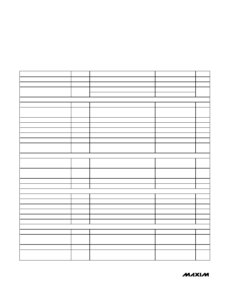
ELECTRICAL CHARACTERISTICS (continued)
(AVDD3.3 = DVDD3.3 = AVCLK = 3.3V, AVDD1.8 = DVDD1.8 = 1.8V, external reference VREFIO = 1.2V, output load 50
double-terminat-
ed, transformer-coupled output, IOUT = 20mA, TA = -40°C to +85°C, unless otherwise noted. Specifications at TA
≥ +25°C are guar-
anteed by production testing. Specifications at TA < +25°C are guaranteed by design and characterization. Typical values are at TA
= +25°C.)
PARAMETER
SYMBOL
CONDITIONS
MIN
TYP
MAX
UNITS
Output Settling Time
To 0.025% of the final value (Note 3)
11
ns
Glitch Impulse
Measured differentially
1
pV
s
IOUT = 2mA
30
Output Noise
NOUT
IOUT = 20mA
30
pA/
√Hz
TIMING CHARACTERISTICS
Input Data Rate
600
MWps
Data Latency
5.5
Clock
cycles
Data to Clock Setup Time
tSETUP
Referenced to rising edge of clock (Note 4)
-1.5
ns
Data to Clock Hold Time
tHOLD
Referenced to rising edge of clock (Note 4)
2.6
ns
Clock Frequency
fCLK
CLKP, CLKN
600
MHz
Minimum Clock Pulse-Width High
tCH
CLKP, CLKN
0.6
ns
Minimum Clock Pulse-Width Low
tCL
CLKP, CLKN
0.6
ns
Turn-On Time
tSHDN
External reference, PD falling edge to
output settle within 1%
350
s
CMOS LOGIC INPUT (PD)
Input Logic-High
VIH
0.7 x
DVDD3.3
V
Input Logic-Low
VIL
0.3 x
DVDD3.3
V
Input Current
IIN
-10
±1.8
+10
A
Input Capacitance
CIN
3pF
LVDS INPUTS
Differential Input High
VIHLVDS
(Notes 6, 7, 8)
+100
+1000
mV
Differential Input Low
VILLVDS
(Notes 6, 7, 8)
-1000
-100
mV
Internal Common-Mode Bias
VICMLVDS
1.125
1.375
V
Differential Input Resistance
RIDLVDS
110
Common-Mode Input Resistance
RICMLVDS
3.2
k
Input Capacitance
CINLVDS
3pF
DIFFERENTIAL CLOCK INPUTS (CLKP, CLKN)
Clock Common-Mode Voltage
CLKP and CLKN are internally biased
AVCLK / 2
V
Minimum Differential Input
Voltage Swing
0.5
VP-P
Minimum Common-Mode Voltage
1V
Maximum Common-Mode
Voltage
1.9
V
发布紧急采购,3分钟左右您将得到回复。
相关PDF资料
MAX5891EGK+D
IC DAC 16BIT LVDS 600MSPS 68-QFN
MAX5893EGK+D
IC DAC 12BIT DUAL 500MSPS 68-QFN
MAX5894EGK+D
IC DAC 14BIT DUAL 500MSPS 68-QFN
MAX5895EGK+D
IC DAC 16BIT 500MSPS DUAL 68-QFN
MAX5898EGK+D
IC DAC 16BIT DUAL 500MSPS 68-QFN
MAX6900ETT+T
IC RTC I2C COMPAT 6-TDFN
MAX6902ETA+T
IC RTC SPI COMPAT 8-TDFN
MAX7375AXR604+T
IC OSC SILICON SC70-3
相关代理商/技术参数
MAX5890EGK+TD
功能描述:数模转换器- DAC 14-Bit 600Msps DAC RoHS:否 制造商:Texas Instruments 转换器数量:1 DAC 输出端数量:1 转换速率:2 MSPs 分辨率:16 bit 接口类型:QSPI, SPI, Serial (3-Wire, Microwire) 稳定时间:1 us 最大工作温度:+ 85 C 安装风格:SMD/SMT 封装 / 箱体:SOIC-14 封装:Tube
MAX5890EGK-D
功能描述:数模转换器- DAC RoHS:否 制造商:Texas Instruments 转换器数量:1 DAC 输出端数量:1 转换速率:2 MSPs 分辨率:16 bit 接口类型:QSPI, SPI, Serial (3-Wire, Microwire) 稳定时间:1 us 最大工作温度:+ 85 C 安装风格:SMD/SMT 封装 / 箱体:SOIC-14 封装:Tube
MAX5890EGK-TD
功能描述:数模转换器- DAC RoHS:否 制造商:Texas Instruments 转换器数量:1 DAC 输出端数量:1 转换速率:2 MSPs 分辨率:16 bit 接口类型:QSPI, SPI, Serial (3-Wire, Microwire) 稳定时间:1 us 最大工作温度:+ 85 C 安装风格:SMD/SMT 封装 / 箱体:SOIC-14 封装:Tube
MAX5890EVKIT#
功能描述:数模转换器- DAC RoHS:否 制造商:Texas Instruments 转换器数量:1 DAC 输出端数量:1 转换速率:2 MSPs 分辨率:16 bit 接口类型:QSPI, SPI, Serial (3-Wire, Microwire) 稳定时间:1 us 最大工作温度:+ 85 C 安装风格:SMD/SMT 封装 / 箱体:SOIC-14 封装:Tube
MAX5890EVKIT-W
制造商:Maxim Integrated Products 功能描述:- Bulk
MAX5891EGK
制造商:Rochester Electronics LLC 功能描述: 制造商:Maxim Integrated Products 功能描述:
MAX5891EGK+D
功能描述:数模转换器- DAC 16-Bit 600Msps DAC RoHS:否 制造商:Texas Instruments 转换器数量:1 DAC 输出端数量:1 转换速率:2 MSPs 分辨率:16 bit 接口类型:QSPI, SPI, Serial (3-Wire, Microwire) 稳定时间:1 us 最大工作温度:+ 85 C 安装风格:SMD/SMT 封装 / 箱体:SOIC-14 封装:Tube
MAX5891EGK+TD
功能描述:数模转换器- DAC 16-Bit 600Msps DAC RoHS:否 制造商:Texas Instruments 转换器数量:1 DAC 输出端数量:1 转换速率:2 MSPs 分辨率:16 bit 接口类型:QSPI, SPI, Serial (3-Wire, Microwire) 稳定时间:1 us 最大工作温度:+ 85 C 安装风格:SMD/SMT 封装 / 箱体:SOIC-14 封装:Tube